Indium phosphide laser on silicon nitride photonic circuit
Researchers based in Belgium and France have used micro-transfer printing (MTP) to integrate indium phosphide (InP) laser gain material on a silicon nitride (Si3N4) photonics platform [Biwei Pan et al, Photonics Research, v12, p2508, 2024].
The team from Ghent University–IMEC in Belgium, Thales Research and Technology in France, IMEC in Belgium and III–V Lab in France reports: “The gain section consists of an aSi:H [amorphous hydrogenated silicon] rib waveguide with an InP coupon micro-transfer-printed on top. A 4μmx840μm gain mesa together with 180μm-long tapers at each side is used to provide sufficient gain for lasing and realize optical coupling between the coupon and aSi:H waveguide.”
Such devices are needed for high-capacity long-haul coherent communication systems, sensors, and microwave photonics. The researchers also see the large tuning range as benefiting large-steering-angle optical phase array (OPA) and high-axial-resolution optical coherence tomography (OCT) systems.
The attractions of the Si3N4 photonics platform over competitors such as silicon-on-insulator (SOI) include much lower propagation losses and much higher on-chip power handling for optical communications. However, the platform is difficult to combine with InP since the optical coupling between the materials is hampered by a large refractive index mismatch. The research team has previously overcome this by using an intermediate hydrogenated amorphous silicon (aSi:H) bridge between the Si3N4 and InP optical fields.
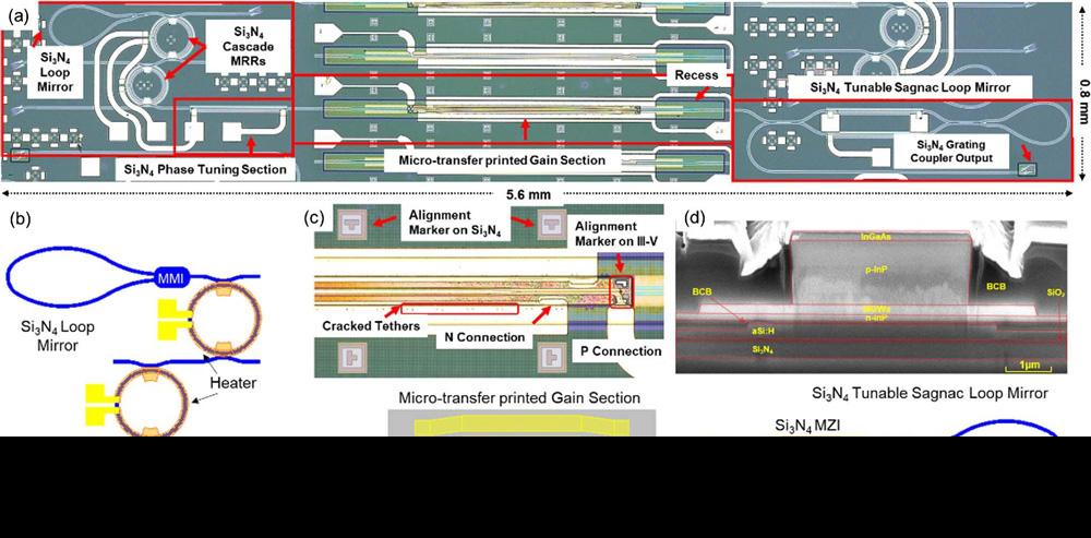
The Si3N4 platform (Figure 1) allowed the researchers to design a tunable laser with an overall chip size of just 5.6mmx0.8mm — “much more compact compared to the laser cavity on the shallow etched silicon waveguide,” according to the team.

Figure 1: (a) Microscope picture of tunable laser. (b) Corresponding schematic diagram of cavity structure (MRR, micro-ring resonator; MMI, multimode interferometer). (c) Zoom-in view of MTP III–V gain section on aSi:H/Si3N4 waveguides. (d) Scanning electron microscope (SEM) cross-section image.
A disadvantage of the Si3N4 platform is a poor thermo-optic coefficient (2.45x10⁻⁵/K), making the usual thermal wavelength tuning of the Si3N4 waveguides more difficult, compared with silicon, requiring extensive simulation and design studies.
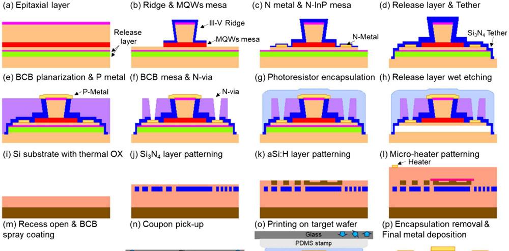
The III-V Lab facility manufactured the InP optical gain structures (Figure 2). The release layers consisted of 50nm indium gallium arsenide (InGaAs) and 150nm indium aluminium arsenide (InAlAs), allowing selective etch against InP.

Figure 2: Schematic process flow of (a)–(h) active coupons on III–V-substrate for micro-transfer printing, and (i)–(m) Si3N4/aSi:H circuits and preparation on the target substrate, and (n)–(p) heterogeneous integration and post-processing.
The fabrication constructed the ridge waveguide and multiple quantum well (MQW) mesa structures. The n-metals were then deposited, followed by pattern and etch down to the release layers. Silicon nitride covered the gain structure and provided tethering of the assembly after the release layers were removed.
The regions between the devices on the wafer was filled with divinylsiloxane–bis-benzocyclobutene (DVS–BCB), and planarized to expose the p-contact region. The p-side metal was applied, and vias to the n-metal contacts made. The DVS–BCB material was also etched to give access to the release layers.
The coupons were then encapsulated with photoresist, and the release layers under-etched using an iron trichloride (FeCl3) water solution, keeping Si3N4 tethers holding the coupon in place.
The researchers comment: “All the III–V-based processes are done on the source wafer, which indicates that different III–V devices can be integrated on the Si/Si3N4-based photonic circuits simultaneously without increasing the process complexity. This advantage is crucial for the Si3N4 platform since it is purely passive and requires all the active building blocks.”
The passive Si3N4 photonic circuits were manufactured at IMEC’s 200mm pilot line. The silicon substrate incorporated a 2.5μm thermal oxide top layer. A 400nm Si3N4 layer was chemical vapor deposited (CVD) at low pressure on top of 700nm high-temperature plasma-enhanced CVD (PECVD) silicon dioxide (SiO2). The Si3N4 photonic circuit was patterned with deep ultraviolet (DUV) photolithography, followed by plasma etch.
A further high-temperature PECVD SiO2 layer covered the photonic structures, followed by planarization to 100nm above the Si3N4 waveguides.
The 330nm amorphous hydrogenated silicon (aSi:H) was also deposited by PECVD, along with a 100nm PECVD Si3N4 hard mask. Rib and strip waveguides were patterned in the aSi:H. The wafer was covered with PECVD SiO2 and planarized. The hard mask material was removed by etch-back.
The photonic wafer was then cleaved into separate samples for further processing. A 50nm aluminium oxide (Al2O3) etch-stop layer was electron-beam evaporated and patterned before a 1.5μm PECVD SiO2 top layer was added. Micro-heaters were created next on top of the photonic structures.
Recesses were made through to the aSi:H structures to enable evanescent coupling. The researchers explain the purpose of the etch-stop material: “The Al2O3 is used as the etch-stop layer to maintain the quality of the surface in the recess for the following bonding process.”
The Al2O3 was removed before a thin 100nm DVS–BCB bonding layer was spray-coated and soft-baked at 150°C. The team comments: “Buildup of the DVS–BCB at the side walls of the recess benefits the following metal connection.”
The researchers used a single-post elastomeric poly-dimethylsiloxane (PDMS) stamp to pick up the 1260μmx45μm III–V coupons for MTP to the photonic circuit.
The team comments: “Although a single-post stamp was used in this experiment, printing of multiple devices at the same time can be realized by using a dedicated stamp with multiple posts.”
Alignment of the coupons to the target position was made through digital pattern recognition markers on both material structures.
The bond was made after removal of the photoresist encapsulation through curing the DVS–BCB at 280°C. The material was found to shrink some 80nm during the curing process. The final wiring was achieved by depositing and patterning a thick layer of titanium/gold (Ti/Au) after removal of DVS–BCB residues.
The team comments: “During printing and post-printing processing, there are neither processes for source and target materials, nor processes requiring high temperature, which means the source and target wafers can be fully implemented in their own established foundries, which greatly facilitates mass production and time to market.”
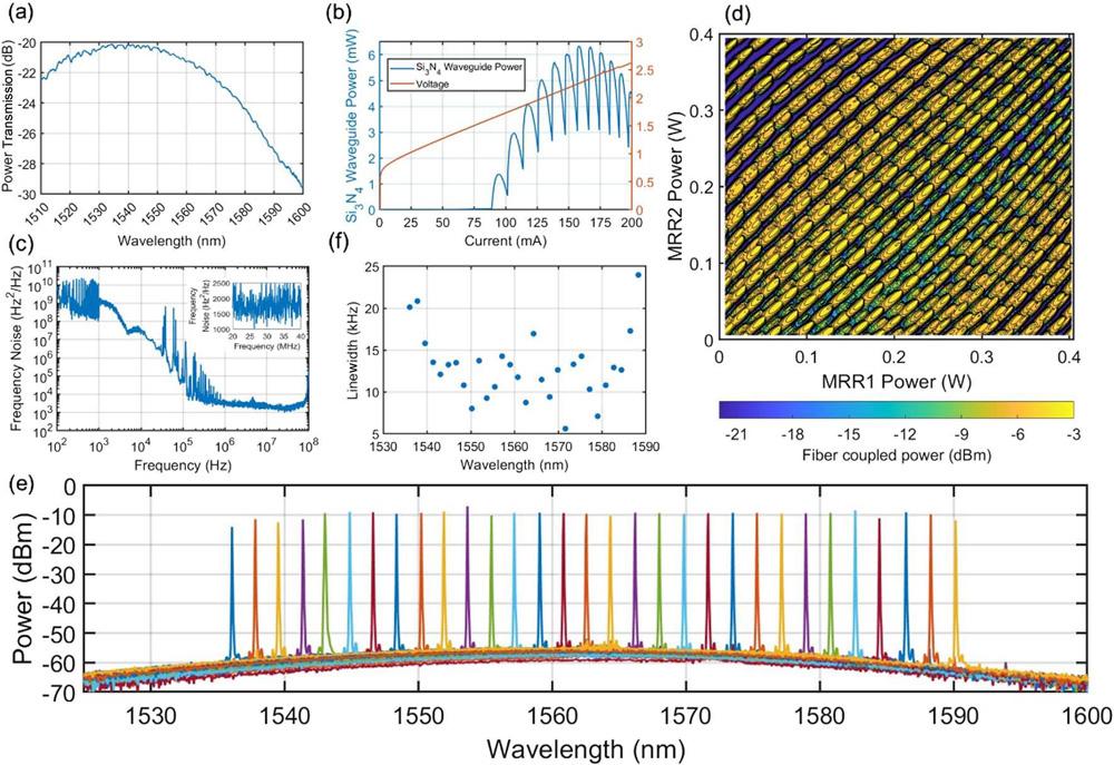
The fabricated laser achieved a 87.6mA threshold with the laser output power reaching 8.3mW at 158.5mA injection (Figure 3). The operating wavelength was 1571.56nm. The temperature was maintained at 15°C using a thermo-electric cooler.

Figure 3: (a) Transmission spectrum of reference waveguide with grating couplers at both sides. (b) Laser light output–current–voltage (LIV) behavior. (c) Frequency noise spectrum at 1571.56nm (inset: zoom-in from 20MHz to 40MHz). (d) Two-dimensional output power tuning map. (e) Optical spectra under different operation wavelengths. (f) Lorentzian linewidths versus wavelength.
The researchers comment: “As the gain section sits on a thick buried oxide layer, thermal roll over starts at an electrical power dissipation of around 346mW. The output power could be further improved by reducing the series resistance and the thermal resistance.”
The intrinsic linewidth was 5.6kHz, according to white-noise-limited frequency measurements. “This linewidth can be influenced by the deviations of the MRR’s self-power coupling ratio, as well as waveguide loss and coupling loss in the experiments,” the team explains.
The wavelength-tuning effects of the MRR heaters was mapped out at 158.5mA. The researchers comment: “The variation in the output power originates from how well the spectra of the MRRs and the cavity modes are aligned to each other at the setpoints. The local peaks in the tuning map occur at precise alignment, which were extracted as the working points of the laser. The laser can be locked to such bias points through a feedback loop to get the preferred working conditions.”
The tuning range was 54nm with more than 40dB side-mode suppression ratio (SMSR). The linewidth was less than 25kHz across this range. The wavelengths fall in the conventional/C (1530–1565nm) and long/L (1565–1625nm) fiber-optic bands. The free spectral range (FSR) was extended beyond the usual Vernier value for two MRRs of about 25nm to three periods. Further extension is presently blocked due to gain bandwidth limitations.
The Sagnac loop enabled reflectivity adjustment of the laser output by applied power input to the micro-heaters changing the optical phase difference between the Mach-Zender interferometer (MZI) sections.


