Selecting the right power MOSFET for your DC-DC converter can improve efficiency and minimize heating.
The ability to charge not just phones but tablets, laptops, earbuds, smartwatches, and other devices from an automobile is a very convenient advancement made possible by USB PD (Power Delivery) technology. One way to implement USB PD technology for charging devices—such as those shown in Figure 1—is to use an H-bridge buck-boost DC power supply that can adjust to the power requirements of these devices.

Figure 1. A single USB connection can charge multiple devices when PD technology is implemented. Image used courtesy of Pixabay
This article presents a design for just such a power supply and evaluates the conversion efficiency and temperature effects using two different automotive power MOSFET options.
USB PD in Automobiles
The USB PD standard presents an approach to USB charging that allows each device to negotiate the voltage and current it receives based on its preferred power requirements. It is classified as a fast-charging technology and is based on the USB Type-C standard—a connector that addresses the evolving needs of platforms and devices. USB Type-C is reversible and supports scalable power and performance, making it future-proof.
USB PD provides a number of benefits, such as reducing the number of chargers and cords an individual needs for their devices. Because it is considered fast charging, the USB PD standard also makes it easier to quickly charge critical devices.
USB PD applications in automobiles are not limited to charging devices but also include powering vehicle accessories and providing backup power. The ability to charge and power devices within an automobile using a single type of cord (USB Type-C) is extremely convenient, and the demand for its inclusion in vehicle designs is rapidly growing. However, as alluded to earlier, successfully integrating USB PD technology in an automobile requires a compatible DC-DC converter.
Buck Boost DC-DC Converters
A Buck-Boost DC-DC converter takes a variable DC input voltage and creates a constant DC output voltage that may be either lower or higher than the input voltage. The buck converter provides a DC voltage step-down, while the boost converter provides a DC voltage step-up.
When using USB PD in automotive applications, the power comes from the automobile battery, and the power-receiving device determines the output voltage. Therefore, the DC-DC converter for automotive USB PD must be a buck-boost converter to create the output voltage from the vehicle battery voltage.
Figure 2 shows the basic configuration of a generic buck-boost DC-DC converter.
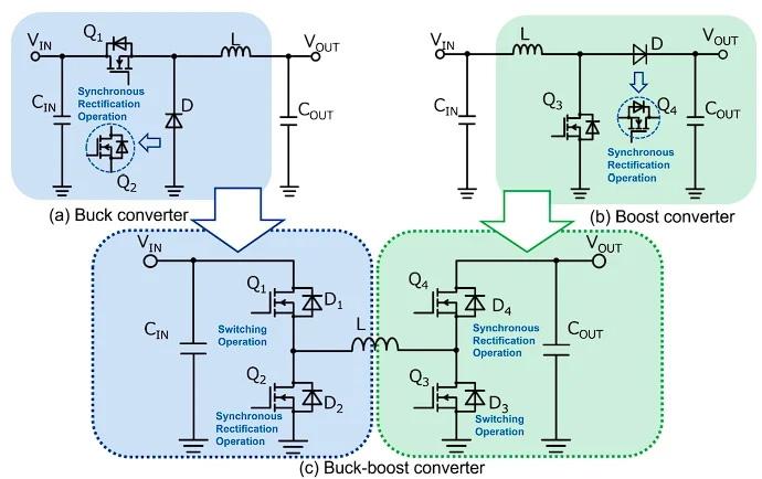
Figure 2. Configuration of a buck-boost DC-DC converter
There are three operating modes for this DC-DC converter:
- Buck Mode, when the input voltage is higher than the desired output voltage
- Boost Mode, when the input voltage is lower than the desired output voltage
- Buck-Boost Mode, when the input voltage is approximately equal to the output voltage and the output voltage fluctuation becomes large in buck or boost mode
Table 1 provides details on how the different portions of the design of Figure 2 work as a function of the operating mode.
Table 1. Buck-boost converter operating mode
|
Mode |
Q1 |
Q2 |
Q3 |
Q4 |
Synchronous Rectifier |
|
Buck |
Switching |
Off |
On |
Q2 |
|
|
Boost |
On |
Off |
Switching |
Q4 |
|
|
Buck-Boost |
Buck Mode |
Boost Mode |
|||
H-Bridge Power Supply with a Buck-Boost DC-DC Converter
An H-bridge is a circuit comprising four switches arranged in two pairs of diagonally opposed switches, with the inductor placed between the switches. This circuit gets its name from the H-shaped topology. At the center of Figure 2 (c), the configuration of the devices to create the H shape is readily apparent.
Challenges for USB PD Automotive Power Supplies
The three main challenges of a USB PD automotive power supply implementing a buck-boost DC-DC converter are efficiency, temperature, and size. Efficiency is always a concern with power supplies, especially with the growing electric and hybrid vehicles industry.
Temperature impacts performance and can increase the cooling requirements. Space, too, is at a premium as automakers seek to optimize the space available to passengers and minimize the space required for automotive electronics.
These challenges can be addressed using the right automotive MOSFETs in the H-bridge buck-boost DC-DC converter.
Buck-Boost Converter Design Case Study
Experimental Design
Figure 3 is the circuit schematic used for the design comparison testing. In the H-bridge section of the design, two different automotive, AEC-Q101 qualified, power MOSFETs from Toshiba were used in this experiment.
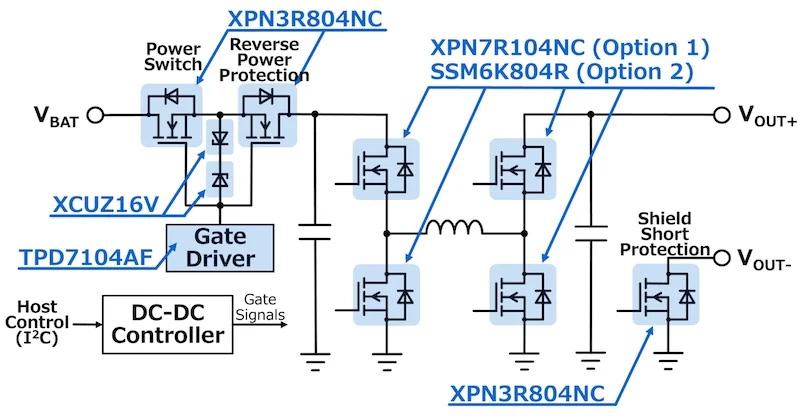
Figure 3. Automotive buck-boost DC-DC converter circuit schematic
The specifications for the automotive USB PD buck-boost converter are provided in Table 2. This H-bridge buck-boost circuit provides the maximum value of 60 W output power for input voltages from 5 to 18 VDC and output voltages from 3.3 to 21 VDC.
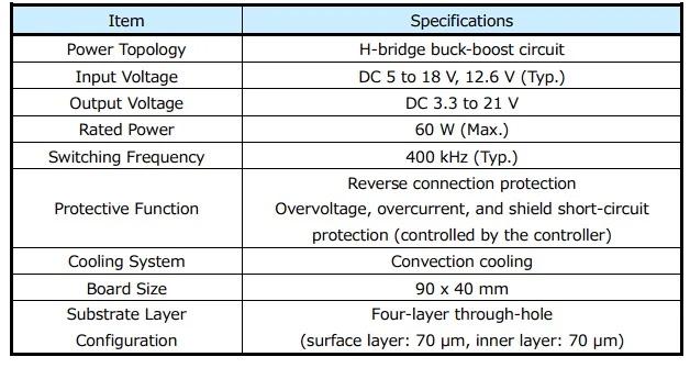
Table 2. USB PD buck-boost converter specifications
Circuit Components
For the testing, the two switching N-channel silicon MOSFETs compared are the:
- Toshiba XPN7R104NC
- Toshiba SSM6K804R
The specifications for these two automotive power MOSFETs are summarized in Table 3.
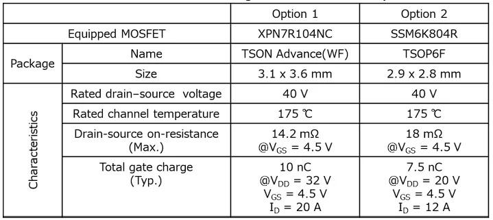
Table 3. Comparison of the two types of MOSFETs used in the buck-boost DC-DC converter
There are two major differences between these MOSFET types: the drain-source on-resistance and the total gate charge. Option 1 has a 14.2 mΩ resistance and a 10 nC gate charge, while Option 2 has a higher level of resistance at 18 mΩ but a lower gate charge at 7.5 nC.
In addition to the two MOSFETs under evaluation, the power supply includes a Toshiba XPN3R804NC automotive power MOSFET that was used as a switching device in the reverse-connection protection circuit and in the shield short-circuit protection circuit. The gate driver for the power switch and reverse-connection protection is the TPD7104AF. In addition, the controller IC is a MAX25432 manufactured by Analog Devices. The remaining components can be found in the BOM provided by Toshiba.
PCB Layout
The assembled USB PD automotive power supply is shown in Figure 4. The overall size of the PCB board is 90 × 40 mm. Both power MOSFETs are compact. The Toshiba SSM6K804R is slightly smaller at 2.9 × 2.8 × 0.82 mm than the Toshiba XPN7R104NC at 3.3 × 3.6 × 0.85 mm.
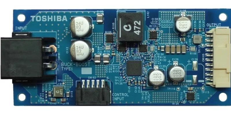
Figure 4. Buck-boost converter power supply
Additional details about the PCB layout including the individual layers can be found in the reference guide from Toshiba.
Performance Comparison for the Two Converter Designs
Power Supply Efficiency
The power supply efficiency was evaluated for each condition (buck, boost, and buck-boost) using both of the MOSFETs. The results are summarized by the measured efficiency curves shown in Figure 5. From this figure, it can be seen that the efficiency varies with the input and output voltages and the load conditions.
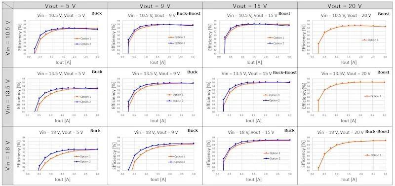
Figure 5. Summary of power supply efficiency results for both types
For light loads, where the output current is small, the switching element experiences small conduction losses and switching losses in higher proportion than other losses. For this type of load, MOSFET Option 2 is more efficient because it utilizes a MOSFET with a smaller gate charge.
For heavy loads, where the output current is large, the power supply experiences a high proportion of conduction losses because of the on-resistance of the switching elements. This makes MOSFET Option 1 the better solution because it utilizes a MOSFET with a smaller on-resistance.
The differences in performance at different loads can be seen more easily in Figure 6. At light loads, Option 2 provides better efficiency. However, as the output current increases, eventually, Option 1 provides better efficiency.
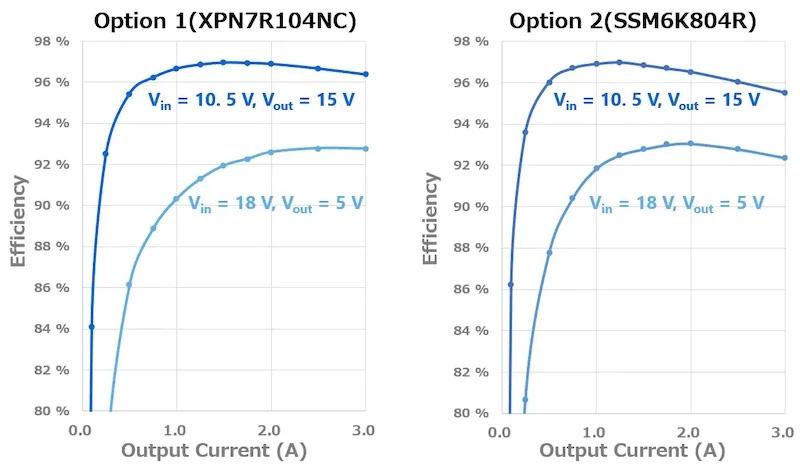
Figure 6. Efficiency curves for the buck-boost converter MOSFET options
Power Supply Temperature
The maximum rated MOSFET channel temperature is 175 °C. If we plan to keep the channel temperature at no more than 80% of its maximum rating, that means we need to limit the transistor temperature to 140 °C.
Given a maximum ambient temperature of 85 °C, the maximum allowable change in temperature becomes 140 - 85 = +55 °C. Figure 7 illustrates the channel temperature change for the Option 1 (Type 1) and Option 2 (Type 2) MOSFETs under various buck and boost mode conditions.
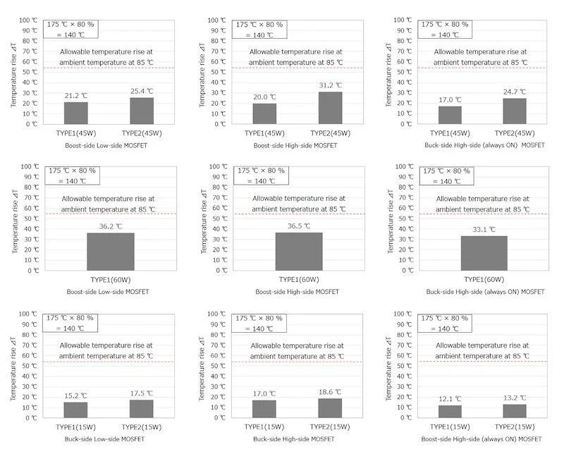
Figure 7. Temperature rise of the MOSFETs in various operating conditions
The highest temperature rise is 36.5 °C as seen in the TYPE1 (60 W) centermost graph of Figure 7. This occurs using the Option 1 MOSFET with the power supply operating in boost mode with a 10.5 VDC input, and a 20 VDC, 3 A output.
Selecting the Right Power MOSFET for Your Automotive Designs
In this article, an experimental design was presented for a USB PD automotive buck-boost DC-DC power supply. Two automotive-grade, N-channel silicon MOSFET options from Toshiba were evaluated: the XPN7R104NC and SSM6K804R.
From this experiment, we can see that tradeoffs can be made between the on-resistance and the gate charge depending on the operating conditions of the buck-boost converter. To learn more about the design presented here, please take a look at the main Reference Design page as well as the Design Guide and Reference Guide.
Toshiba Electronic Devices & Storage has many MOSFET solutions certified for use in automotive designs that support the development of compact designs and that provide high efficiency and excellent thermal performance. These MOSFETs combine state-of-the-art wafer processes that make possible the suppression of switching noise and industry-leading levels of low resistance achieved through packaging technologies.
Contact Toshiba Electronic Devices & Storage today to learn about how their automotive power MOSFETs can revolutionize your USB PD charger design.
Unless otherwise noted, all images used courtesy of Toshiba Electronic Devices & Storage
Industry Articles are a form of content that allows industry partners to share useful news, messages, and technology with All About Circuits readers in a way editorial content is not well suited to. All Industry Articles are subject to strict editorial guidelines with the intention of offering readers useful news, technical expertise, or stories. The viewpoints and opinions expressed in Industry Articles are those of the partner and not necessarily those of All About Circuits or its writers.